Students can Download 2nd PUC Electronics Previous Year Question Paper March 2018, Karnataka 2nd PUC Electronics Question Bank with Answers helps you to revise the complete Karnataka State Board Syllabus and score more marks in your examinations.
Karnataka 2nd PUC Electronics Previous Year Question Paper March 2018
2nd PUC Electronics Previous Year Question Paper March 2018
Time : 3 hrs. 15 min.
Max Marks: 70
Instructions:
- The question has five Parts A, B, C and D.
- Part – A has no choice
- Part – D has two parts. Part -1 is from problems, Part – II is of essay type questions.
- Circuit diagram/timing diagram/truth tables are drawn wherever necessary.
- Problems without necessary formula/formulae carry no marks.
Part – A
Answer all questions: 10 x 1 = 10
Question 1.
Define Pinch off voltage.
Answer:
Pinch off voltage is the drain to source voltage in JFET at which the drain current reaches constant satenation level.
Question 2.
What is the input impedance of an ideal op-amp?
Answer:
Input impedance, Zin = ∞
Question 3.
Mention the number of sidebands present in an AM wave.
Answer:
2 sidebands.
![]()
Question 4.
Define frequency modulation.
Answer:
Frequency modulation is the process in which the frequency of the carrier is varied in accordance with the modulating signal, keeping amplitude and phase of carrier wave constant.
Question 5.
Expand MOSFET.
Answer:
Metal Oxide Semiconductor Field Effect Transistor.
Question 6.
Convert (1001)G to binary code.
Answer:
(1001)G = (1110)2
Question 7.
Draw the symbol of XOR-gate.
Answer:
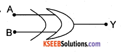
Question 8.
Write the meaning of MOV Rs, A.
Answer:
Copy the content of accumulator (register A) to R5
![]()
Question 9.
If a = 6 and b = 9, what is the content of a after the execution of a+ = b in C programming?
Answer:
a = 6 + 9 = 15
Question 10.
What is cell splitting?
Answer:
Cell splitting is the process of dividing the geographical area into many {smaller areas.
Part – B
Answer any Five questions. 5 x 2 = 10
Question 11.
Derive the relation μ = gm x rd
Answer:
- Ac drain resistance (rd) is the ratio of small change in drain to source voltage VDS to the corresponding change in drain current (ID) for a constant VGS.
- Transconductance (gm) is the ratio of change in drain current ID to the corresponding change in gate to source voltage VGS for a constant VDS.
Question 12.
Mention any two characteristics of CC amplifier.
Answer:
- Voltage gain is nearly equal to 1
- Input and output signals are in phase
Question 13.
Draw the block diagrams of voltage shunt and current series negative feedback.
Answer:
1.Voltage series negative feedback.
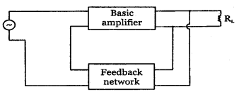
2. Voltage shunt negative feedback:
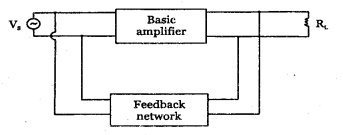
3.Current series negative feedback:
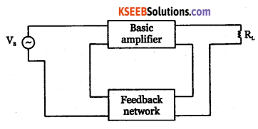
4. Current shunt negative feedback:
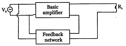
![]()
Question 14.
An amplifier has Z0 = 10KQ, voltage gain A = 150 and P = 0.02. Find the output impedance of feedback amplifier.
Answer:
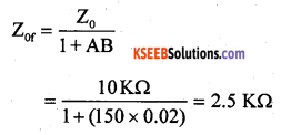
Question 15.
Write the pin diagram of IC-555 timer.
Answer:
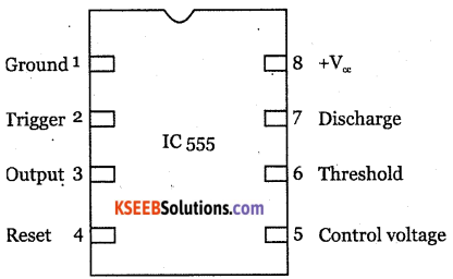
Question 16.
Mention the four modes of operation of TRIAC.
Answer:
A triac can conduct in both the directions. The conduction of a triac is initiated by injecting a current pulse into the gate terminal. The gate loses control over the conduction once TRIAC is turned ON. The TRIAC turns OFF only when the current through the main terminals becomes zero.
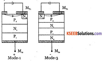
The three terminals of TRIAC are marked MT, (Main terminal 1), MT2 (Main terminal 2) and the gate G. As TRIAC is a bidirectional device and can have its terminals at various combinations of positive and negative voltages, there are four possible electrons potential combinations, as given below:
- MT2 positive with respect to MT1, G positive with respect to MT1.
- MT2 positive with respect to MT1, G negative with respect to MT1.
- MT2 negative with respect to MT1, G negative with respect to MT1.
- MT2 negative with respect to MT1, G positive with respect to MT1.
In trigger mode-1, the gate current IG, flows mainly through P2N2 junction like an ordinary thyristor. When the gate current has injected sufficient charge into P2 layer, the TRIAC starts conducting through the P1, N1, P2, N2, layers like an ordinary thyristor.
In trigger mode-3, the gate current IG forward biases the P2 P3 junction and large number of electrons are introduced in the P2 region by Nr Finally the structure P2 N1, P1, N4 turns on completely.
Question 17.
What is a half subtractor? Write its truth table.
Answer:
Half subtractor.
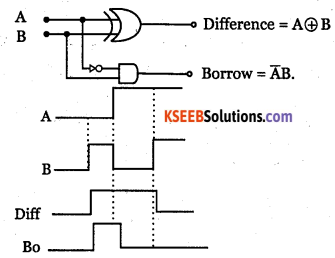
| Inputs | Outputs | ||
| A | B | Difference | Borrow |
| 0 | 0 | 0 | 0 |
| 0 | 1 | 1 | 1 |
| 1 | 0 | 1 | 0 |
| 1 | 1 | 0 | 0 |
![]()
Question 18.
Give any two applications if Wi-Fi.
Answer:
- Wi-Fi is used to access the internet via hotspots with a laptop computer.
- It is one of the most reliable, flexible and affordable wireless networking technology.
- Wi-Fi allows cheaper deployment of local area network in outdoor areas like historical buildings.
- The price of chipsets for Wi-Fi continues to drop, making it an economical networking operation.
- The standard Wi-Fi device will work anywhere in the world.
Part – C
Answer Any FiveQuestions
Question 19.
Define the terms:
(i) Thermal runaway
(ii) Leakage current
(iii) Heat sink.
Answer:
(i) The self destruction of an unbiased transistor due to increase in temparature and hence increase in leakage current is called thermal runaway.
(ii) Leakage current is the current through a device due to the motion of minority charge carriers under reverse biased condition.
(iii) Heat sink is a device which absorbs the unnecessary heat generated in the transistor and radiates it to surroundings and protects it.
Question 20.
Explain the three modes of radio wave propagation.
Answer:
- Ground Waves
- Space Waves
- Skywaves
Question 21.
Draw the equivalent circuit of transmission lines for high frequency. Mention any two uses of microstrip antenna.
Answer:
For low frequency

Primary constants:
- The series resistance per unit length R is proportional to the square root of frequency.
- The inductance L per unit length for a 2 wire T-line is \(\mathrm{L}=\frac{\mu}{2} \log \left(\frac{2 \mathrm{D}}{\mathrm{d}}\right)\) where pt is the permeability.D is distance between two wires. And d is diameter of each wire.
- The capacitance C per unit length,
\(C=\cfrac{\mu}{\log \frac{2 D}{d}}\) - Where e is the permittivity of free space, D is distance between 2 wires and d is the distance between the plates of capacitor.
Secondary constants of T-line:
- The series impedance of T-line is Z=R+jwL.
- The shunt admittance of T-line is y=G+JWC are the two secondary constants.
Question 22.
Explain the operation of power diode under forward biased condition.
Answer:
Power diodes of largest power rating are required to conduct several kilo amps of current in the forward direction with very little power loss while blocking several kilovolt in the reverse direction. Large blocking voltage requires wide depletion region. Charge density in the depletion layer should also below in order to get a wide depletion region. For these two requirements, drift layer is introduced between two heavily doped p and n layers.
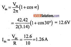
\(\mathrm{V}_{\mathrm{m}}=\sqrt{2} \mathrm{V}_{\mathrm{rms}}=\sqrt{2} \times 30=42.42 \mathrm{V}\)
Question 23.
Determine Vdc and Idc of SCR half wave rectifier. Given firing angle is 30° and rms voltage of ac input to the rectifier is 30V and load is 10Ω.
Answer:
Question 24.
Mention any three features of PIC microcontroller.
Answer:
24/35 I/O pins with individual direction control:
- High current source/sink for direct LED drive
- Interrupt-on-Change pin
- Individually programmable weak pull-ups
- Ultra Low-Power Wake-up (ULPWU)
Analog Comparator module with:
- Two analog comparators
- Programmable on-chip voltage reference (CVREF) module (% of VDD)
- Fixed voltage reference (0.6V)
- Comparator inputs and outputs externally accessible
- SR Latch mode
- External Timer 1 Gate (count enable)
A/D Converter:
- 10-bit resolution and 11/14 channels
- Timer O: 8-bit timer/counter with 8-bit programmable prescaler
Enhanced Timer 1:
- 16-bit timer/counter with prescaler
- External Gate Input mode
- Dedicated low-power 32 kHz oscillator
Timer2: 8-bit timer/counter with 8-bit period register, prescaler and postscaler
![]()
Enhanced Capture, Compare, PWM+ module:
- 16-bit Capture, max. resolution 12.5 ns
- Compare, max. resolution 200 ns
- 10-bit PWM with 1, 2 or 4 output channels, programmable “dead time”, max. frequency 20 kHz
- PWM output steering control
Capture, Compare, PWM module:
- 16-bit Capture, max. resolution 12.5 ns
- 16-bit Compare, max. resolution 200 ns
- 10-bit PWM, max. frequency 20 kHz
Enhanced USART module:
- Supports RS-485, RS-232, and LIN 2.0
- Auto-Baud Detect
- Auto-Wake-Up on Start bit
- In-Circuit Serial Programming TM (ICSPTM) via two pins
- Master Synchronous Serial Port (MSSP) module – supporting 3-wire SPI (all 4 modes) and 12C™ Master and Slave Modes with I2C address mask
![]()
Question 8.
Briefly explain different addressing modes in the 8051.
Answer:
There are four addressing modes in 8051.
- Immediate addressing mode: the data source is available immediately as a part of instruction itself. Example: MOV A, #8bit data
- Register addressing mode: the source and destination register names are parts of the opcode in instruction. Example: MOV A, R0
- Direct addressing mode: the source and/or destination may be the internal RAM locations. Example: MOV 90h, #50h
- Indirect addressing mode: the source or destination address may be indicated the content of index register. Example: MOV @Rl,#40h
Question 25.
For a 8-bit computer, if A = 0000 0101 and B = 0011 0100. Compute the following bitwise operators.
(i) A & B
(ii) A | B
(iii) A ∧ B
Answer:
A&B = 0000 0100 A | B = 0011 0101 A∧B = 0011 0001
Question 26.
Explain with diagram, the working of a satellite transponder system.
Answer:
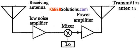
Part – D
Answer any Three question 3 x 5 = 15
Question 27.
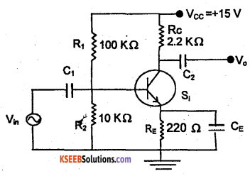
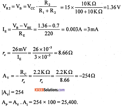
For the CE amplifier using silicon transistor given below, calculate
(i) Voltage across R2
(ii) Emitter current IE
(iii) Voltage gain Av
(iv) Power gain Ap Given that \(r_{e}^{\prime}=\frac{26 \mathrm{mV}}{\mathrm{I}_{\mathrm{E}}} \text { and } \beta=100\)
Answer:
Question 28.
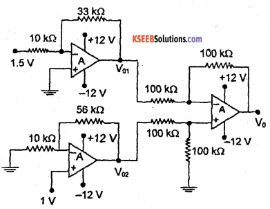
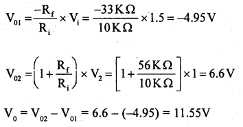
Calculate output voltage V0for the circuit given below.
Answer:
Question 29.
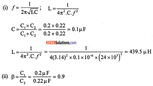
A Colpitts oscillator circuit generates a frequency of 24 KHz. The capacitors used in the tank circuit are Ct = 0.2pF and C2 = 0.22pF. Calculate the value of an inductor L and feedback factor β.
Answer:
![]()
Question 30.
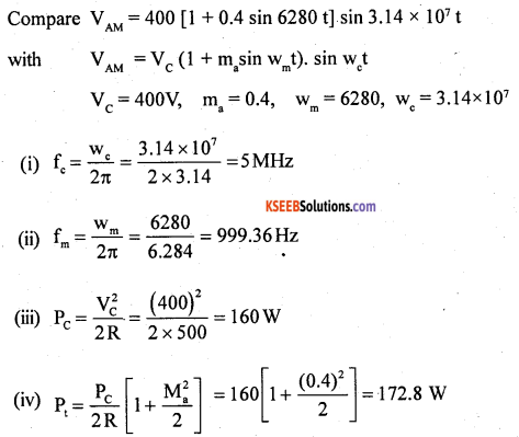
The output of an AM transmitter is given by 400[1 + 0.4 sin(6280) t] sin(3.14 x 10⁷f). This voltage is fed to an antenna of resistance 500Ω. Determine
- Carrier frequency
- Modulating frequency
- Carrier power
- Mean power output.
Answer:
Question 31.
Simplify the Boolean expression Y =∑m (0,2,6,8,10,12,13,14) + ∑d (4,9) using K-map. Draw the NAND-gate equivalent circuit to realize the simplified expression.
Answer:

Part – E
Answer any Four questions. 4 x 5 = 20
Question 32.
Draw the circuit diagram of two stage RC-coupled amplifier. Explain its frequency response.
Answer:
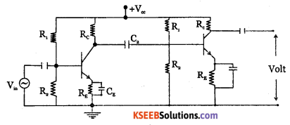
RC coupling is most widely used method of coupling signal from one stage to next stage in multistage amplifiers. The two stage RC coupled amplifier is as shown in the diagram. The signal developed across the collector resistor Rc of the first stage is capacitively coupled to the input of second stage through the coupling capacitor Cc.
RC coupled transistor amplifier is widely used as it provides excellent audio fidelity over wide range of frequency.
R1R2,Rc,RE provide biasing resistors. RE provides stabilisation and CE is used for bypassing ac across Rg.
Working:
When an AC signal is applied to the input of first stage, it gets amplified and appears at its output with a phase reversal of 180°. Through the coupling capacitor Cc, the amplified signal is fed to the input of second stage.
Cc blocks DC and allows AC to pass through. The second stage further amplifies the signal, further providing a phase reversal of 180° with respect to its input. The input and output signal are in phase as the signal is reversed twice. Overall gain of RC coupled amplifier is the product of gain of individual stages.
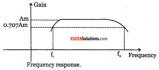
At low frequencies, reactance of coupling capacitor is high. Hence it allows only a small part of the signal to pass from one stage to next stage. Hence gain is low at low frequencies. At high frequencies, the coupling capacitor Cc offers low reactance and acts like a short. Hence loading effect of next stage increases and the gain decreases.
In mid frequency range, as frequency increases, the capacitive reactance of coupling capacitor decreases, which tries to increase gain. As capacitive reactance decreases, due to loading effect of next stage, the gain reduces. Hence, voltage gain is constant.
![]()
Question 33.
What is an integrator? With circuit diagram, obtain an expression for output voltage of an op-amp integrator.
Answer.
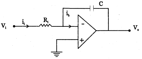
Integrator is a circuit whose output is proportional to integral of its input.
Question 34.
With a labelled block diagram explain the working of FM superhetrodyne radio receiver.
Answer:
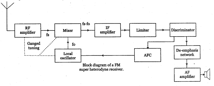
when turned to the desired frequency. The RF amplifier is designed to handle large bandwidth of 150 kHz.
Mixer: the incoming RF signal of frequency fm is applied to a mixer which also receives the output from the local oscillator. A new frequency called intermediate frequency IF is produced whose value is difference of local oscillator signal f and signal frequency f.
Local oscillator: the receiver converts incoming carrier frequency to the IF by using local oscillator frequency higher than incoming tuned frequency. Colpitts oscillator is used as the local oscillator.
IF amplifier: IF signal is amplified by one or more number of amplifiers, which raises the strength of IF signal. It has multistage class A amplifier providing better selectivity and gain.
Limiter: It removes all the amplitude variation in FM signal caused by noise. Differential amplifiers are preferred for limiter.
Discriminator: It recovers the modulating signal from the IF signal. It converts frequency variation into corresponding voltage variation and produces the modulating signal. De-emphasis network: It reduces the relative amplitude of high frequency signals that are boosted in the transmitter and brings them back to their original level.
AF amplifier: It amplifier the modulating signal recovered by the FM detector. The speaker converts the electrical signal into sound signal.
Question 35.
(a) What is a register? Mention the different types of shift registers.
Answer:
- Serial-in, serial-out.
- Serial-in, parallel-out
- Parallel-in, serial-out.
- Parallel-in, parallel-out.
(b) Draw the logic diagram of clocked SR flip-flop.
Answer:

It is constructed using inverters inserted into inputs of cross coupled NAND gates.
Working:
- When S=0, R=0, it does not respond and hence outputs Q and Q will remain in their previous state. This is called HOLD condition.
- When S=1 and R=0, the output Q and Q change to 1 and 0. This condition is called SET state.
- When S=0, R=1, the output Q and Q change to 0 and 1. This condition is called RESET state.
- When S=1 and R=l, it drives output Q and Q both to HIGH which is FORBIDDEN or INVALID condition.

Question 36.
Write an assembly language program to subtract 23 H from 3 F H when CY = 0 and save the result in Rs.
Answer:
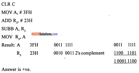
![]()
Question 37.
Write a C program to accept the radius of a circle and compute its area and perimeter.
Answer:
# include < stdio.h>
# include <conio.h>
void main ( )
{
float radius, area, perimeter, PI = 3.142; clrscr ( );
printf (“Enter the radius\n”); scanf (“%f’, & radius);
Area = PI * radius * radius;
Perimeter = 2.0 * PI * radius;
printf (“Area of circle is % f \n”, Area);
printf (“perimeter of the circle is % f \n”, perimeter); getch ( );
}