Karnataka 1st PUC Electronics Question Bank Chapter 8 Introduction to Digital Electronics
One Mark Questions and Answers
Question 1.
What is a digital signal?
Answer:
A Digital signal is a signal which can have only two distinct values.
Question 2.
What is a bit?
Answer:
The bit is a binary digit that can be either 0 or 1.
![]()
Question 3.
What is a nibble?
Answer:
A nibble is a group of four bits.
Question 4.
What is a byte?
Answer:
A byte is a group of eight bits.
Question 5.
What is meant by the base or radix of a number system?
Answer:
The base or radix of a number system is the number of distinct symbols used in the number system.
Question 6.
How many basic symbols are used in (i) binary (ii) hexadecimal (iii) decimal number systems?
Answer:
- Two
- Sixteen
- Ten.
Question 7.
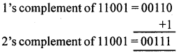
Write l‘s complement of binary number 11001.
Answer:
00110.
![]()
Question 8.
What is 2’s complement of a binary number 11001?
Answer:
Question 9.
What is a logic gate?
Answer:
A logic gate is a digital circuit that makes logical decisions.
Question 10.
What type of gate is obtained when two switches are (i) in parallel (ii) in series?
Answer:
- OR gate
- AND gate.
![]()
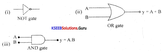
Question 11.
What are (i) NOT gates (ii) OR gates and (iii) AND gates?
Answer:
- NOT gate is a logic circuit whose output is a complement or negation of the input.
- OR gate is a logic circuit whose output is LOW only when all its inputs are LOW.
- AND gate is a logic circuit whose output is HIGH only when all its inputs are HIGH.
Question 12.
Draw the logic symbols of (1) NOT gate (ii) OR gate and (iii) AND gate?
Answer:
Two Mark Questions and Answer
Question 1.
Distinguish between analog and digital signals.
Answer:
Analog systems are systems that are capable of processing a continuous range of values varying with respect to time.
Digital systems are systems that process discrete values.
![]()
Question 2.
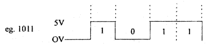
Write examples for (I) bit (ii) nibble (iii) byte.
Answer:
- Bit: 0 or I.
- Nibble: 1100
- Byte: 11000101
Question 3.
Perform binary addition of the numbers, 11002 + 11112.
Answer:

Question 4.
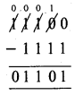
Perform binary subtraction of the number 111002 – 11112.
Answer:
![]()
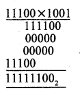
Question 5.
Perform binary multiplication of the number 111002 × 10012.
Answer:
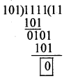
Question 6.
Perform binary division of the number 11112 by 1012.
Answer:
Question 7.
What is the decimal equivalent of DAD16?
Answer:
DAD16 = 13 × 162 + 10 × 161 + 13 × 16°
= 13 × 256 + 160+ 13
= 3328 + 160 + 13
= 350110
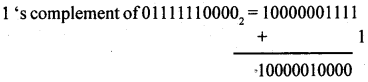
Question 8.
Find the 2’s complement of the binary number 011111100002.
Answer:
![]()
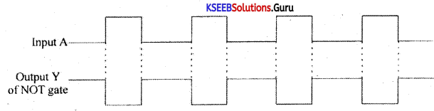
Question 9.
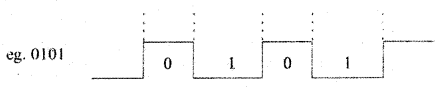
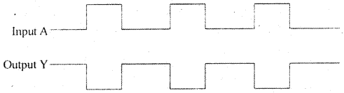
What is a timing diagram? Sketch the timing diagram of NOT gate.
Answer:
The timing diagram is a pictorial representation of inputs and output states of a logic circuit
Question 10.
What are positive logic and negative logic?
Answer:
In positive logic, HIGH or 1 represents a higher voltage level and LOW or 0 represents a lower voltage level.
In negative logic, LOW or 0 represents a higher voltage level and HIGH or 1 represents a lower voltage level.
Positive logic is widely used in all digital applications and negative logic is rarely used.
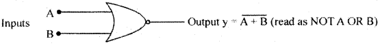
Question 11.
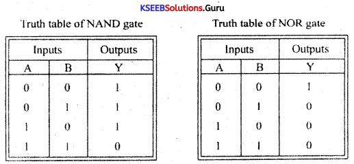
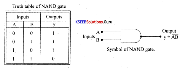
What is a NAND gate? Draw its circuit symbol.
Answer:
NAND gate is a logic circuit whose output is LOW only when all its inputs are HIGH.
![]()
Logic symbol of NAND gate
![]()
Question 12.
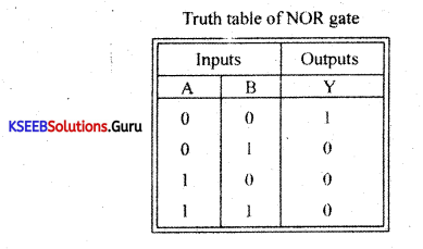
What is NOR gate? Draw its logic symbol.
Answer:
NOR gate is a logic circuit whose output is HIGH only when all its inputs are LOW.
Logic symbol of NOR gate
Question 13.
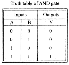
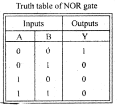
Write the truth tables of NAND gate and NOR gate.?
Answer:
Question 14.
What are the least significant bit and most significant bit?
Answer:
The leftmost bit of a binary number that has the highest place value is called the most significant bit. The rightmost bit of a binary number that has the least place value is called the least significant bit.
Question 15.
What are the advantages of the binary number system and a hexadecimal number system?
Answer:
It is easy to design digital electronic circuits that operate with only two digits in a binary number system to represent two voltages in digital circuits, it is used in digital circuits.
The hexadecimal number system is used to express large binary numbers more concisely.
![]()
Question 16.
Define (i) weight or place value (ii) truth table.
Answer:
Weight or place value is the definite value that is assigned to each position in a number. The truth table gives the output of a logic gate for different combinations of its inputs.
Three Mark Questions and Answers
Question 1.
Draw the two input diode OR gate and write its truth tables?
Answer:
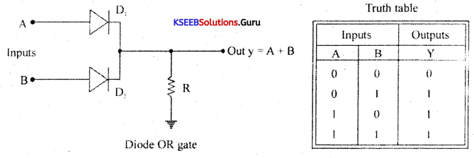
Question 2.
Define nibble and byte with an example for each.
Answer:
A nibble is a group of four bits
eg. 1010,1001.
A byte is a group of eight bits.
eg. I 01 01 00 I, 1000 1110,
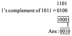
Question 3.
Subtract 10112 from 11012 using 1 ‘s complement method.
Answer:
NOT
![]()
Question 4.
Show that A+ ĀB = A + B.
Answer:
LHS = A + ĀB
= A(1) + Ā B = A(1+B) + Ā B {QA = A.l}
=A + AB + ĀB
= A +AB + Ā B
= A + B (A + Ā)
= A+B.I {QA + Ā = 1}
= A + B {QB.1 = B}
= RHS.
Question 5.
Simplify Y = ABC(AB̅ + AC̅)+ AB̅C (AB̅ + AC̅)+ A
Answer:
Y= ABC(AB̅ +AC̅)+ AB̅C(AB̅ + AC̅) + A
= ABC.AB̅ + ABC.AC̅ + AB̅C.AB + AB̅C.AC̅ + A
= 0 + 0 + 0 + 0 + A = A
Question 6.
Prove that A + BC = (A + B). (A + C).
Answer:
RHS = (A+ B) (A+ C)
= A.A + AC + BA + BC
= A + AC + BA+ BC (QA.A = A)
= A(1 +C) + BA + BC
= A. 1 +BA + BC. (Q 1 +C = I)
= A+ BA + BC (Q A.1 = A)
= A(1 + B)+ BC
= A.1 + BC (Q1 + B = I)
= A + BC
= LHS
![]()
Question 7.
Simplify y = \(\overline{(\mathbf{A}+\overline{\mathbf{B}}) \cdot(\overline{\mathbf{C}}+\mathbf{D})}\)
Answer:
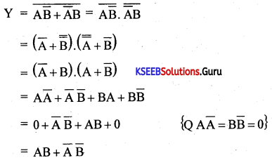
Question 8.
Simplify y = \(\overline{(\mathbf{A}+\overline{\mathbf{B}})(\overline{\mathbf{C}}+\mathbf{D})}\)
Answer:
y = \(\overline{(\mathrm{A}+\overline{\mathrm{B}}) \cdot(\overline{\mathrm{C}}+\mathrm{D})}\)
= \(\overline{(\mathrm{A}+\overline{\mathrm{B}})}+\overline{(\overline{\mathrm{C}}+\mathrm{D})}\)

Question 9.
Simplify y = ABC+ A+ ABCD + CD
Answer:
y = ABC + A + ABCD + CD
= A(BC + 1) + ABCD + CD .
= A1 + ABCD + CD (Q1 + A = 1)
= A + ABCD + CD
= A(1 +BCD).CD
= A.I + CD
= A + CD {A.1 = A}
Question 10.
Write any three advantages of digital electronics.
Answer:
- Accuracy and precision are very high.
- Information storage and design are easy.
- Large digital circuits can be fabricated on IC chips.
![]()
Question 11.
Convert (i) (F02)16 into decimal and (ii) (11011012) into decimal number.
Answer:
(i)(F02)6 = F × 162 + 0 × 16 + 2 × 16°
= 15 × 256 + 0 + 2 × 1
= 3840 + 0 + 2 = (3842)10
(ii) (11011012) = 1 × 26 + 1 × 25 + 0 × 24 + 1 × 23 + 1 × 22+ 0 × 21 +1 × 2°
= 1 × 64 + 1 × 32 + 0 + 1 × 8 + 1 × 4 + 0 + 1 × 1
= 64 + 32 + 8 + 4 + 1
= (109)10
Question 12.
Draw the circuit of the DTL NOR gate and write its truth table.
Answer:
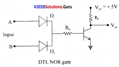
DTL NOR gate
Five Mark Questions and Answers
Question 1.
Subtract (27)10 from (56)10 using 2’s complement method.
Answer:
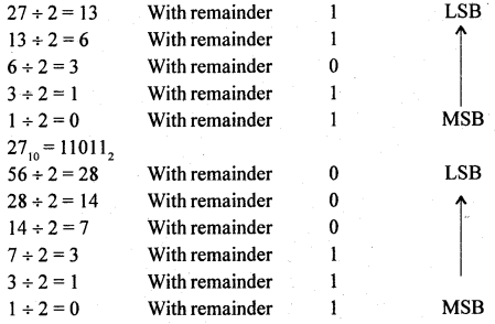
5610 = 1110002
Minuend → 111000
Subtrahend → 0110011
After disregarding end carry, the answer is 111012
![]()
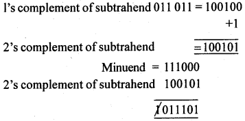
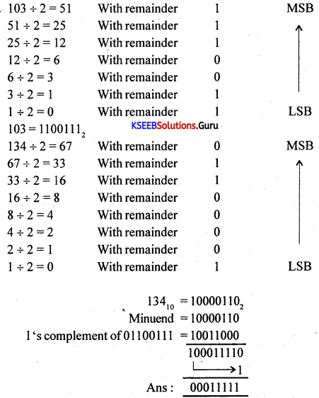
Question 2.
Subtract (103)10 from (134)10 using 1 ‘s complement method.
Answer:
Question 3.
Explain the transistor NOT gate
Answer:
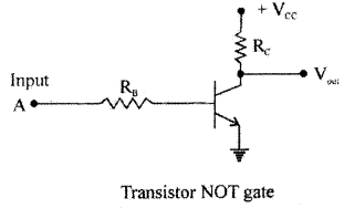
Working:
Case (i) When the input is LOW, the base-emitter junction has no forward bias applied and hence base and collector currents become zero. The transistor is driven to cut off and it acts as an open switch. Hence the output at the collector becomes HIGH.
![]()
Case (ii) When the input is HIGH, base-emitter junction is forward biased and hence base and collector currents flow driving the transistor to saturation. Hence output at the collector becomes
LOW.
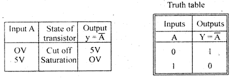
The timing diagram of NOT gate
Question 4.
Explain the action of a two-input diode AND gate.
Answer:
AND gate is a logic gate that produces a HIGH output only when all its inputs are HIGH.
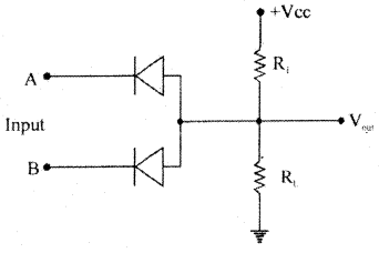
Working:
Case (i) When A = 0, B = 0, both the diodes are forward biased and act like closed switches. Hence all the applied voltage drops across R, and the output voltage becomes LOW.
Case (ii) When A = 0, B = 1, diode D1 conducts as it is forward biased and diode D2 does not t conduct as it is reverse biased. Hence all the applied voltage drops across R, and the output voltage becomes LOW.
Case (iii) When A= 1, B = 0, diode D1, does not conduct but D2 conducts being forward biased. Hence all the applied voltage drops across R, and the output voltage at y becomes LOW.
![]()
Case (iv) When A = I, B = 1 both diodes are reverse biased and do not conduct. No current flows through R and hence no voltage drop across R. Hence output at y becomes HIGH.
Question 5.
Explain the action of two input diode OR gates.
Answer:
OR gate is a logic circuit whose output is LOW only when all its inputs are LOW.
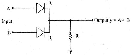
Case (i) When A = 0, B = 0, both the diodes are not conducting. No current flows through resistor RL and hence output y = 0.
Case (ii) When A = 0, B = 1, D1, is reverse biased and does not conduct. D2 is forward biased and conducts. Hence current flows through RL making output y = 1.
Case (iii) When A = 1, B = 0, D1, conducts as it is forward biassed, and D2 does not conduct as it is reverse biased. The current flows through RL and output y = I.
Case (iv) When A = 1, B = 1, both the diodes conduct as they are forward biased. The current flows through RL making output y HIGH.
Question 6.
Explain the action of two input DTI NAND gates.
Answer:
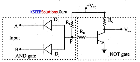
Case (i) When both inputs A and B are LOW (OV), both the diodes D1 and D2 are forward biased. Hence voltage at junction P of the diode becomes zero. This makes the transistor Q go to cut off. Hence the output at the collector of the transistor becomes HIGH.
Case (ii) When A is LOW and B is HIGH, D1 is forward biased and D2 is reverse biased. Hence the voltage at P becomes zero. This makes the transistor go to a cut-off state and therefore output at its collector becomes HIGH.
Case (iii) When A is HIGH and B is LOW, D1 is reverse biased and D2 is forward biased due to which voltage at Pis zero. This makes the transistor go to a cut-off state and therefore output at its collector becomes HIGH.
![]()
Case (iv) When both the inputs are HIGH, D1 and D2 are reverse biased. Hence voltage at P becomes +VCC. This makes the transistor Q go to saturation and the transistor acts like a closed switch. Therefore output becomes LOW.
Question 7.
Explain the working of the DTL NOR gate.
Answer:
NOR gate is a logic circuit whose output is HIGH only when both its inputs are LOW
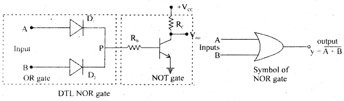
Diodes D1 and D2 form OR gates and the transistor act as NOT gate.
Case (i) When A = 0, B = 0, the diodes are not forward biased and they do not conduct. – Hence voltage P is zero. This zero voltage makes the transistor go to cut-off condition and therefore output is HIGH.
Case (ii) When A= 0, B = 1, D1 does not conduct but D2 conducts. Hence voltage at P is +VCC and it drives the transistor to saturation and output becomes LOW.
![]()
Case (iii) When A = 1, B = 0, D1 conducts and D2 does not conduct. Hence voltage at P is +VCC and this makes the transistor Q go to saturation. Hence output becomes LOW.
Case (iv) When A = 1, B = 1, both diodes conduct as they are forward biased. Then voltage at P is +VCC and the transistor is driven to saturation. The output at the collector becomes LOW.
Question 8.
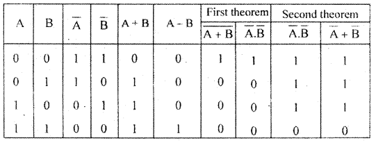
State and prove De Morgan’s theorems.
Answer:
First theorem: The complement of a logical sum is equal to logical product of complements \(\overline{\mathrm{A}+\mathrm{B}}\) = A̅.B̅
Second theorem: The complement of a logical product is equal to the logical sum of complements.
\(\overline{\mathrm{AB}}\) = A̅ + B̅
Proof:
Question 9.
Explain the working of IC LM555 as a clock pulse generator.
Answer:
IC LM555 timer is a transistor logic integrated circuit. It is used to generate clock waveform to digital circuits. It is called an astable multivibrator because neither of its two distinct states is stable.
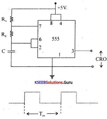
The frequancy of oscillation f = \(\frac{1.44}{\left(R_{A}+2 R_{B}\right) C}\)
![]()
Question 10.
Explain the working of a monostable pulse generator using IC S55.
Answer:
The circuit diagram of the monostable pulse generator is as shown below:
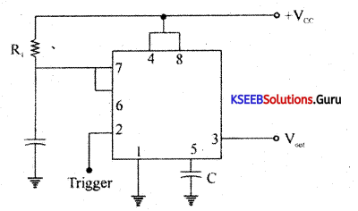
When the trigger input falls below \(\frac{1}{3}\)Vcc, the capacitor begins to charge and the output becomes
HIGH. When the voltage across capacitor exceeds\(\frac{2}{3}\)Vcc, it discharged and output returns to a LOW stable state.
The output remains in LOW state until another trigger pulse falls below \(\frac{\mathrm{V}_{\mathrm{CC}}}{3}\)and the cycle repeats.