Students can Download 2nd PUC Electronics Chapter 2 Transistor Biasing Questions and Answers, Notes Pdf, 2nd PUC Electronics Question Bank with Answers helps you to revise the complete Karnataka State Board Syllabus and score more marks in your examinations.
Karnataka 2nd PUC Electronics Question Bank Chapter 2 Transistor Biasing
2nd PUC Electronics Transistor Biasing One Mark Questions and Answers
Question 1.
What is biasing of a transistor?
Answer:
Tranistor biasing is the application of suitable DC voltages across the transistor terminals.
Question 2.
Why is the transistor called as current controlled device?
Answer:
The output current of a transistor depends upon the input current. Hence, the transistor is called as current controlled device.
Question 3.
What is an unbiased transistor?
Answer:
A transistor with its terminals not connected to any source is called an unbiased transistor.
![]()
Question 4.
Define quiescent point.
Answer:
The zero signal collector current and collector to emitter voltage is called quiescent point.
Question 5.
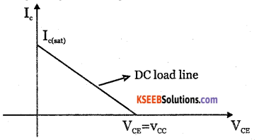
What is meant by dc load line?
Answer:
Dc load line is a straight line drawn on the output characteristics representing output DC voltage and corresponding direct current under no signal conditions.
Question 6.
What is thermal runaway?
Answer:
The self destruction of an unbiased transistor due to increase in temparature and hence increase in leakage current is called thermal runaway.
Question 7.
Define stabilisation of a transistor.
Answer:
Stabilisation of a transistor is the process of making. Q point independent of transistor parameters and temparature variations.
Question 8.
Mention any one factor on which stabilisation depends.
Answer:
stabilisation depends upon β.
Question 9.
Name any one parameter of the transistor which is temparature dependent.
Answer:
Leakage current
Question 10.
What is leakage current?
Answer:
Leakage current is the current through a device due to the motion of minority charge carriers under reverse biased condition.
![]()
Question 11.
Mention any one leakage current in a transistor.
Answer:
Collector to emitter current with the base open ICEO.
Question 12.
Name anyone biasing circuit.
Answer:
Fixed bias.
Question 13.
Name the biasing circuit which gives excellent stabilisation.
Answer:
Voltage divider biasing circuit.
Question 14.
What is a heat sink?
Answer:
Heat sink is a device which absorbs the unnecessary heat generated in the transistor and radiates it to surroundings and protects it.
Question 15.
Write the relation between ICE0 and ICB0.
Answer:
ICEO = (I+p)ICBO.
2nd PUC Electronics Transistor Biasing Two Marks and Three Marks Questions and Answers
Question 1.
Explain the biasing of a transistor.
Answer:
The application of suitable DC voltage across the transistor terminals is called biasing of the transistor.
The reasons for biasing of a transistor are:
- To make the operating point to be at the centre of the load line.
- To make the collector current independent of temperature variations.
- To maintain the operating point constant even though transistor is replaced by another of same type.
![]()
Question 2.
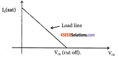
Draw the DC load line and mark the endpoints.
Answer:
Question 3.
Mention any two biasing circuits.
Answer:
- Fixed bias
- Collector to base feedback.
Question 4.
What are the quiescent point and load line?
Answer:
Operating point is the zero signal values of collector Ic and collector to emitter voltage VCE of a transistor. DC load line is a straight line drawn on the output characteristics representing output DC voltage and corresponding direct current under no signal conditions.
Question 5.
Why is the voltage divider bias circuit preferred in the amplification process?
Answer:
The operating point does not depend upon the value of β of the transistor. Hence the operating point does not change its position due to rise in temperature or replacing a transistor of different p value. Hence voltage divider bias provides excellent stabilisation and is preferred to other biasing methods.
Question 6.
What is leakage current? Mention different types of leakage currents.
Answer:
Leakage current is current through a device due to the motion of minority charge carriers under reverse bias conditions.
Different leakage currents are:
- Collector to base leakage current with emitter open (ICBO).
- Collector to emitter leakage current with base open (1CEO).
![]()
Question 7.
What are advantages of voltage divider bias?
Answer:
- Q point gets stabilised very well as the stabilication factor does not
depend upon p. - It provides better amplification when used in amplifiers.
Question 8.
What is the significance of load line?
Answer:
Load line is a straight line drawn on output characteristics representing output DC voltage and corresponding output direct current under no signal condition. Load line contains every possible operating point for the circuit.
Question 9.
Explain the collector to base leakage current and collector to emitter leakage current.
Answer:
1. The current flowing through the collector when the emitter terminal is open is called collector to base leakage current with emitter open ICB0. This leakage current doubles for every 10°c rise in temperature. This leakage current also increases when the reverse bias voltage is increased.
2. The current flowing through the collector when base terminal is open is called collector to emitter leakage current with base open.This current increases with increase in temperature. This leakage current increases when the reverse bias voltage is increased.
Question 10.
What is thermal runaway? Explain.
Answer:
The self destruction of an unbiased transistor due to increase in temperature and hense increase in leakage current.
![]() ‘
‘
Question 11.
On what factors does stabilisation of a transistor amplifier depend upon?
Answer:
The value of p and temperature.
Question 12.
What is meant by heat sink? Mention its importance.
Answer:
Heat sink is a device which absorbs unwanted heat generated in the transistor and radiates to the surroundings. A copper conductor with different shapes are connected to the device to take out heat from the device. With heat sink, power rating of the device increases.
Question 13.
What is unbiased transistor? Explain the need for biasing the transistor.
Answer:
Unbiased transistor is a transistor with its terminals not connected to any source. Biasing a transistor is applying a suitable DC voltage across the transistor terminals to operate the transistor in the desired region.
Need for biasing a transistor are:
- To make operating point to be at the centre of load line for faithful amplification.
- To make collector current independent of temperature variations.
- To make operating point stabilised even when one transistor is replaced by another.
Question 14.
Describe the steps to draw dc load line for a transistor.
Answer:
Consider the equation VCE = Vcc-Ic x Rc)
To plot the point on x-axis, put I =0 in equ (1)
VCE = Vcc
To plot the point on y-axis, put VCE=0, in equ (1)
eqn(1) = ICsat \(=\frac{V_{C C}}{R_{C}}\)
The load lines is drawn joining these end points
Question 15.
What is voltage divider bias? Mention its advantages.
Answer:
Voltage divider bias is the method of biasing a transistor. The voltage drop across forword biases the base emitter junction. This causes the base current and hence collector current to flow in zero signal condition and establishes operating point.
Advantages:
- It offers excellent stabilisation and hence Q point does not shift.
- when used in amplifiers, it provides better amplification.
![]()
Question 16.
Explain the steps required to draw the dc load line for voltage divider bias.
Answer:
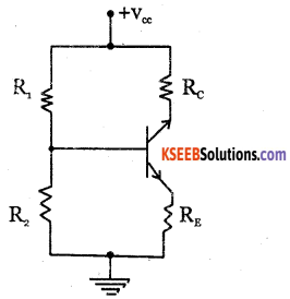
Applying KVL to the circuit,
Vcc= IcRe + Vce + IcRe
Vcc =Ic(Rc+Re)+ Vce.
Vcc=Vcc – Ic(Rc+Re) ……………….. (1)
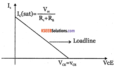
To plot the point on x axis, put Ic =0.
Equ (1) becomes, VCE = VCC
To plot the point on y axis, put VCE=0.
Equ (1) becomes,
\(\mathrm{I}_{c}=\frac{\mathrm{V}_{c c}}{\mathrm{R}_{c}+\mathrm{R}_{\varepsilon}}\)
DC load line is drawn from the end points and is plotted as shown below:
Question 17.
Name the different biasing circuits. Which biasing circuit is better recommeded to get faithful amplification?
Answer:
Different biasing circuits are:
- Fixed bias
- collector to base bias.
- Emitter feedback bias.
- Voltage divider bias.
voltage divider biasing circuit is the best method to get faithful amplification.
2nd PUC Electronics Transistor Biasing Five Marks Questions and Answers
Question 1.
Derive the expressions for the Q point in voltage divider bias.
Answer:
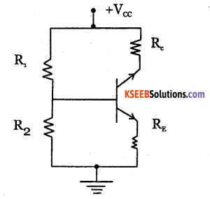
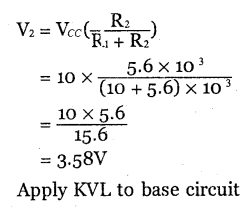
Voltage across R2 is
\(\mathrm{V}_{2}=\frac{\mathrm{V}_{C C} \mathrm{R}_{2}}{\mathrm{R}_{1}+\mathrm{R}_{2}}\)
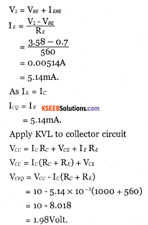
Applying KVL to the base circuit , We get
V2 = VBE + V2
V2 = VBE + IE RE
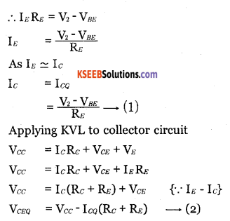
Equations 1 and 2 define operating point or Q point.
![]()
Question 2.
How does stabilisation takes place in voltage divider bias? Explain
Answer:
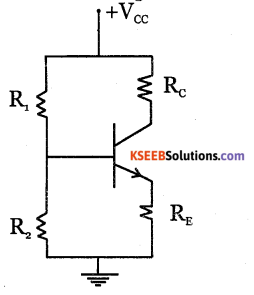
From voltage divider theorem, voltage across the resistor R2 is \(\mathrm{Y}=\mathrm{A} \overline{\mathrm{C}} \overline{\mathrm{D}}+\overline{\mathrm{B}} \mathrm{D}+\overline{\mathrm{A}} \mathrm{D}+\mathrm{BC} \overline{\mathrm{D}}\)
Apply KVL to base emitter loop
V2 =VBE + VE
V2 = VBE = IE RE
VBE = V2 – IE RE
Whenever Ic increases, due to increase in β or temperature, the current IE also increases (IE=IC). Hence IE RE increases and VBE decreases due to which base current IB decreases. Decrease in L decreases Ic and thus the operating point gets stabilised.
Question 3.
Find the end points of the load line for the circuit given below:
Answer:
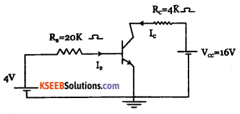
Applying KVL to collector circuit, We get,
Vcc =IcRc + Vce
16 =Ic x 4 x 10³+Vce …………. (1)
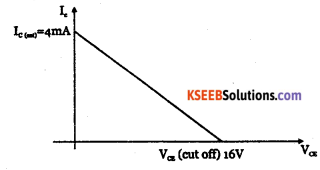
Put Ic = 0 in equation (1), we get,
VCE ( cut off)
= Vcc
= 16 V
This is cut off point on the x-axis.
Put VCE = 0 in equation (1), we get,
16 = IC x 4 x 10³+ 0, IC = 16 x 10-3 /4 = 4mA.
This is saturation point on y axis
Question 4.
Applying KVL to collector circuit, we have
Answer:
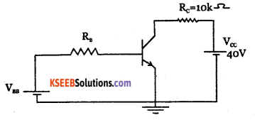
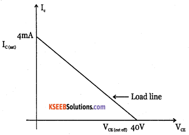
Applying KVL to collector circuit, We get,
Vcc = icRe+VCE
40 = Ic x 10 x 103+Vce …………(1)
Put Ic =0,
40 = VCE (cut off)
This is cut off point on x-axis.
![]()
Question 5.
Draw the load line for the following circuit:
Answer:
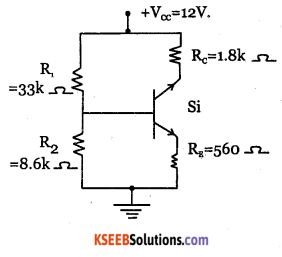
Question 6.
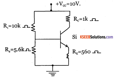
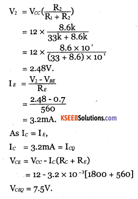
Find the operating point of the circuit given below:
Answer:
