Students can Download 2nd PUC Electronics Chapter 1 Field Effect Transistor (FET) Questions and Answers, Notes Pdf, 2nd PUC Electronics Question Bank with Answers helps you to revise the complete Karnataka State Board Syllabus and score more marks in your examinations.
Karnataka 2nd PUC Electronics Question Bank Chapter 1 Field Effect Transistor (FET)
2nd PUC Electronics Field Effect Transistor (FET) One Mark Questions and Answers
Question 1.
What is FET?
Answer:
Field effect transistor is a three-terminal device in which the flow of current is controlled by an applied electric field.
Question 2.
Expand the term FET.
Answer:
FET stands for Field Effect Transistor.
Question 3.
Is FET a current controlled device or a voltage controlled device?
Answer:
FET is a voltage controlled device.
Question 4.
Name the terminals of FET?
Answer:
Gate, Drain, and Source.
![]()
Question 5.
What are the two main types of FET?
Answer:
- Junction field effect transistor (JFET).
- Metal oxide semiconductor field effect transistor (MOSFET) or Insulated gate field effect transistor (IGFET).
Question 6.
Expand JFET.
Answer:
Junction Field Effect Transistor.
Question 7.
Expand MOSFET.
Answer:
Metal oxide semiconductor Field Effect Transistor.
Question 8.
Expand IGFET.
Insulated Gate Field Effect Transistor.
Question 9.
Mention two types of JFET.
Answer
- Junction FET
- Metal oxide semiconductor FET.
Question 10.
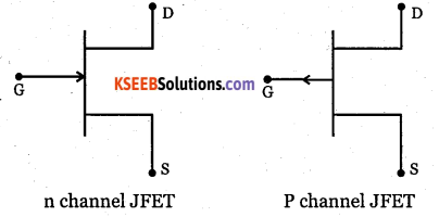
What is an n channel JFET?
Answer
In channel FET has n type semiconductor bar with two p type heavily doped regions diffused on opposite sides.
![]()
Question 11.
What is P channel JFET?
Answer
p channel FET has p type semiconductor bar with two n type heavily doped regions diffused on opposite sides.
Question 12.
How many pn junctions are present in JFET?
Answer
Two pn junctions.
Question 13.
What is the function of the gate?
Answer
Gate controls the flow of charge carriers through the channel.
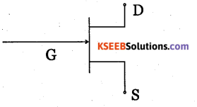
Question 14.
Draw the symbol of n-channel JFET.
Answer:
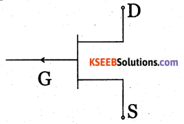
Question 15.
Draw the symbol of p channel FET.
Answer:
Question 16.
Is FET a unipolar device or bipolar device?
Answer
Unipolar device.
Question 17.
Name the charge carriers that are responsible for the conduction of current in a n-channel JFET?
Answer
Free electrons.
![]()
Question 18.
Name the charge carriers that are responsible for the conduction of current in p-channel JFET.
Answer
Holes.
Question 19.
Write the function of the source.
Answer
Source supplies charge carriers for conduction.
Question 20.
What is the function of drain?
Answer
Drain collects the charge carriers supplied by the source.
Question 21.
Which is the type of potential usually applied to the gate terminal?
Answer
Negative potential.
Question 22.
What is pinch off voltage?
Answer
The negitive gate voltage at which drain current becomes zero.
Question 23.
What is the value of drain current at pinch off condition?
Answer
Zero.
Question 24.
Name any two characteristics of JFET.
Answer
- Drain characteristics
- Transfer characteristics.
What are drain characteristics?
Answer
Drain characteristics is set of curves drawn for the relationship between drain current (ID)
and drain to source voltage (VDS) at a constant gate to source voltage (VGS).
![]()
Question 26.
What are transfer characteristics?
Answer
These are the set of curves drawn for the relationship between drain current (ID) and gate to source voltage (VGS) at a constant drain to source voltage (VDS).
Question 27.
What is drain resistance?
Answer
The drain resistance is the ratio of drain to source voltage VDS to the drain current ID for a constant value of gate to source voltage VGS.
Question 28.
What is transconductance?
Answer
It is the ratio of change in drain current ID to the corresponding change in gate to source voltage VGS for a constant drain to source voltage VDS.
Question 29.
What is the amplification factor?
Answer
It is the ratio of change in drain to source voltage VDS to a corresponding change in gate to source voltage VGS for constant drain current ID.
Question 30.
Write the relation between p, rd, and gm.
Answer
u = rd x gs
Question 31.
What is IDSS?
Answer
IDSS is the drian to source saturation current.
![]()
Question 32.
Write any one characteristic feature of FET.
Answer
FET is voltage controlled device.
2nd PUC Electronics Field Effect Transistor (FET) Two Marks Questions and Answers
Question 1.
Expand the terms FET and MOSFET.
Answer:
FET= Field Effect Transistor
MOSFET= Metal oxide semiconductor Field Effect Transistor.
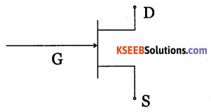
Question 2.
Draw the circuit symbol of n-channel FET and name the terminals.
Answer:
Question 3.
Write the functions of drain and gate.
Answer:
Drain collects the charge carriers supplied by the source. Gate controls the flow of charge carriers through the channel.
Question 4.
Draw the symbols of n-channel and p-channel JFET.
Answer:
Question 5.
Write any two differences between JFET and BJT.
Answer:
| FET | BJT |
| It is a voltage controlled device. | It is a current controlled device. |
| It is a unipolar device. | It is a bipolar device. |
![]()
Question 6.
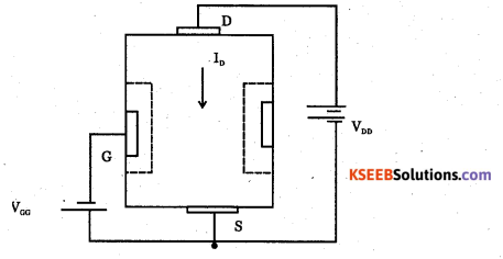
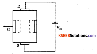
Describe briefly the construction of n-channel JFET.
Answer:
FET can be fabricated with either n-channel or p-channel. For fabricating n-channel FET, first a narrow bar of n type semiconductor material is taken and then two pn juntions are diffused on opposite sides of its middle part.
These junctions form two pn junctions and area between these gate is called channel. The two p regions are internally connected and a single lead is brought out which is called gate terminal. Ohmic contacts are made at the two ends of the bar called source terminals and the other drain terminal D.
Question 7.
Describe briefly the construction of p-channel JFET.
Answer:
For fabricating p-channel FET, first a narrow bar of p type semiconductor material is taken and then two pn junctions are diffused on opposite sides of its middle part. These junctions form two pn junctions and area between these gates is called the channel.
The two p regions are internally connected and a single lead is brought out which is called gate terminal. Ohmic contacts are made at the two ends of the bar called source terminals and the other drain terminal D.
![]()
Question 8.
Name the charge carriers in the current conduction of n-channel and p-channel JFETs.
Answer:
N channel FET has free electrons as charge carriers and p channel FET has holes as charge carriers.
Question 9.
Explain what happens to the pn junctions when the gate is reverse biased?
Answer:
When the gate is reverse biased, the depletion regions are extended towards the channel by the application of reverse bias voltage. When VGS= OV, is when gate terminal is open, the drain current is maximum and flows from drain to source called LDss . If VGs is increased, the reverse bias across the junction increases reducing the width of the channel.
This makes the drain current decrease. Further increase in the reverse bias voltage widens the depletion region and the drain current ID further decreases. Thus the drain current in the device is mainly controlled by the reverse voltage applied across the gate-to-source voltage.
Question 10.
What is pinch off? What is the value of drain current at pinch off?
Answer:
Pinch off voltage is the gate voltage at which the drain current is zero.
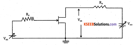
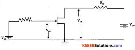
Question 11.
Draw the circuit diagram to plot the charcteristics of n-channel JFET.
Answer:
Question 12.
Explain the terms rd and gm.
Answer:
- Ac drain resistance (rd) is the ratio of small change in drain to source voltage VDS to the corresponding change in drain current (ID) for a constant VGS.
- Transconductance (gm) is the ratio of change in drain current ID to the corresponding change in gate to source voltage VGS for a constant VDS.
![]()
Question 13.
What is amplification factor? Write its relation with rd and gm.
Answer:
Amplification factor is the ratio of small change in drain source voltage to the corresponding change in gate to source voltage for a constant drain current.
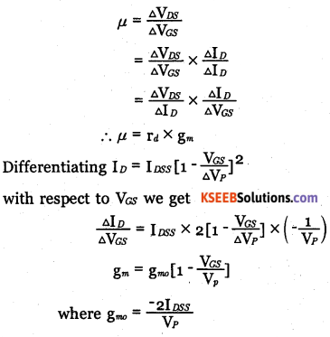
μ = rd gm
Question 14.
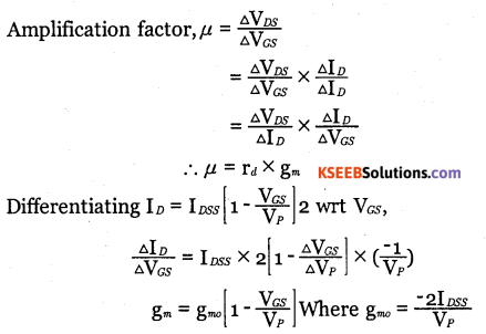
Derive the relation μ = rd x gm
Answer:
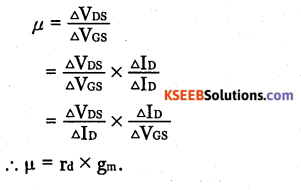
Question 15.
What is IDSS? Write the relation between ID, IDSS, VGS and Vp,IDSS is drain to drain to source saturation current.
Answer:
IDSS is drain to drain to source saturation current.
\({ I }_{ { D } }={ I }_{ { DSS } }\left[ 1-\frac { { V }_{ { GS } } }{ { Vp } } \right]\)
![]()
Question 16.
What is transconductance? Write the relation between gm,gmo ,VGs, and Vp
Answer:
Transconductance is the ratio of small change in drain current (ID) to the corresponding change in gate to source voltage (VGS) for a constant drain to source voltage.
\(g_{m}=g_{m o}\left[1-\frac{V_{G S}}{V_{P}}\right]\)
2nd PUC Electronics Field Effect Transistor (FET) Three Marks Questions and Answers
Question 1.
Define the terms
(a) amplification factor
(b) transconductance and
(c) drain resistance
Answer:
(a) Amplification factor is the ratio of change in drain to source voltage to corresponding change in gate to source voltage for a constant drain current.
(b) Transconductance is the ratio of change in drain current to corresponding change in gate to source voltage for a constant drain to source voltage.
(c) Drain resistance is the ratio of change in drain to source voltage to corresponding change in drain current for a constant gate to source voltage.
Question 2.
Derive the relation μ = rd x gm and gm = gmo \(\left[1-\frac{V_{c s}}{V_{p}}\right]\)
Answer:
Question 3.
Compare BJT and JFET.
| S.No. | BJT | JFET |
| 1. | It is a bipolar device. | It is a unipolar device. |
| 2. | It is a current controlled device. | It is a voltage controlled device. |
| 3. | Current conduction is by both holes and electrons. | Current conduction is by holes or electrons. |
| 4. | Input resistance is low. | Input resistance is very high. (MCI) |
| 5. | BJT is more noisy. | JFET is less noisy. |
| 6. | Switching speed is less. | Switching speed is high. |
| 7. | Fabrication in IC is difficult. | Fabrication in IC is simpler. |
![]()
Question 4.
Explain the working of n channel JFET.
Answer:
Consider n channel JFET with gate to source voltage VGG and drain to source voltage VGG. When VGG is zero, drain current is maximum and flows from drain to source called as Lcc. When V0G is increased, reverse bias across junction increases and width of depletion region across the junctions increases. Due to this channel width decreases and hence the drain current decreases. Thus the reverse voltage applied across gate to source terminal controls the drain current. When the gate to source voltage is further increased, a stage will be reached at which two depletion regions touch each other and the drain current becomes zero. Pinch off voltage is the gate voltage at which drain current becomes zero.
Question 5.
Explain the characteristics of n channel JFET with a circuit diagram.
Answer:
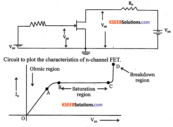
Drain characteristics: It gives the relation between drain current and drain to source voltage at a constant gate to source voltage.
Ohmic region: From O to A, in the ohmic region, drain current is directly proportional to drain to source voltage.
Saturation or pinch off region: From A to B, drain current increases slowly with increase in drain to source voltage. The curve from B to C is the saturation region in which the drain current remains a constant.
Curve from C to D is the breakdown region. In this region, drain current increases rapidly with the increase in drain to source voltage.
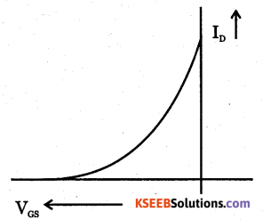
2. Transfer characteristics: It gives the relation between drain current and gate to source voltage for a constant drain to source voltage. Keeping VDS constant, VGS is varied and corresponding ID are nated. The graph obtained is shown:
2nd PUC Electronics Field Effect Transistor (FET) Five Marks Questions and Answers
Question 1.
Explain the classification of FET and the construction of a n-channel JFET.
Answer
The two types of FET are: ‘
- Junction field effect transistor. (JFET)
- Metal oxide semiconductor field effect transistor (MOSFET) or Insulated Gate field Effect transistor (IGFET).
FET can be fabricated with either n-channel or p-channel. For fabricating n-channel FET, first a narrow bar of n-type semiconductor material is taken and then two pn juntions are diffused on opposite sides of its middle part. These junctions form two pn junctions and area between these gate is called channel. The two p regions are internally connected and a single lead is brought out which is called gate terminal. Ohmic contacts are made at the two ends of the bar called source terminal s and the other drain terminal D.
![]()
Question 2.
Distinguish between FET and BJT.
Answer
| FET | BJT. |
| 1. It is unipolar device. | 1. It is a bipolar device. |
| 2. It is a voltage controlled device. | 2. It is a current controlled devices. |
| 3. Its input resistance is very high. | 3. Input resistance is very low. |
| 4. Current conduction is only by majority charge carriers either hole or electron. | 4. Current conduction is both by electrons and holes. |
| 5. It has high switching speed. | 5. It has low switching speed. |
| 6. Less noisy | 6. More noisy. |
| 7. Fabrication is easier in IC. | 7. Difficult to fabricate in IC. |
Question 3.
Explain the formation of depletion regions due to gate potential and also drain-source voltage.
Answer:
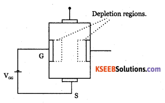
Consider an n-channel FET. The pn junctions are formed by the n-channel and p-type gate. These pn junctions are always reverse biased.
The two pn junctions are reverse biased by source VGG.
As the pn junctions are reverse biased, there will be only immobile positve and negative ions near the pn junction which is called depletion region. The extension of depletion region of n.
channel FET is heavily doped, the depletion region extends more towards n region. The reverse bias on there pn junctions can also be achieved by applying a voltage across source and drain. The source VDD is applied across drain to source. The drain to source voltage produces reverse bias across the gate-source junction. VDD makes the electrons flow from the source to drain through the channel and circuited. This reverse bias creates depletion regions within the channel.
Question 4.
Explain the characteristics of n channel JFET with a circuit diagram.
Answer:
Drain characteristics: It gives the relation between drain current and drain to source voltage at a constant gate to source voltage.
Ohmic region: From O to A, in the ohmic region, drain current is directly proportional to drain to source voltage.
Sturation or pinch off region: From A to B, drain current increases slowly with increase in drain to source voltage. The curve from B to C is the saturation region in which the drain current remains a constant.
Curve from C to D is the breakdown region. In this region, drain current increases rapidly with the increase in drain to source voltage.
Circuit to plot the characteristics of n-channel FET.
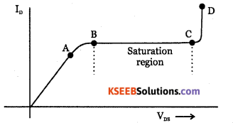
Drain characteristics: It gives the relation between drain current and drain to source voltage at a constant gate to source voltage.
Ohmic region: From O to A, in the ohmic region, drain current is directly proportional to drain to source voltage.
Sturation or pinch off region: From A to B, drain current increases slowly with increase in drain to source voltage. The curve from B to C is the saturation region in which the drain current remains a constant.
Curve from C to D is the breakdown region. In this region, drain current increases rapidly with the increase in drain to source voltage.
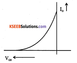
Transfer characteristics: It gives the relation between drain current and gate to source voltage for a constant drain to source voltage. Keeping VDS constant, VGS is varied and corresponding ID are nated. The graph obtained is shown in the diagram.
![]()
Question 5.
Explain the terms ID, Inss, gm, gmo & μ.
Answer
Id = Drain current
IDss = Drain to source saturation current,
gs = Transconductance
\(\mathbf{g}_{m o}=\frac{-2 I_{D S S}}{V_{P}}\)
Where Vp is the pinch off voltage.
μ = amplification factor.
Question 6.
Derive the relation μ = rd X gm and gmo = { g }_{ { mo } }\left[ 1-\frac { { V }_{ { GS } } }{ { V }_{ { P } } } \right]
Answer:
Problem with Solutions
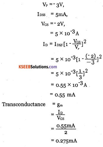
Question 1.
The pinch-off voltage of FET is-3v and drain saturation current is 5mA. It the gate to source voltage is-2v, find the values of drain current and transconductance of the FET.
Answer:
![]()
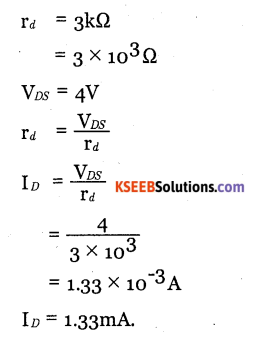
Question 2.
Find the value of drain current if drain resistance rd= 3kQ, and drain to source voltage is 4v when the gate terminal is open.
Answer:
Question 3.
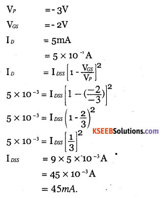
The pinch off voltage of FET is – 3v. For a gate to source voltage – 2v, the drain current is 5mA. Calculate the drain to source saturation current.
Answer:
Question 4.
Find the value of μ given rd =5kΩ, gm =12ms
Answer:
rd= 5kQ = 5 x 10³ Ω
gm = 12 ms = 12 x 10-3S
μ = rm x gm
= 5 x 103 x 12 x 10-3
μ = 60
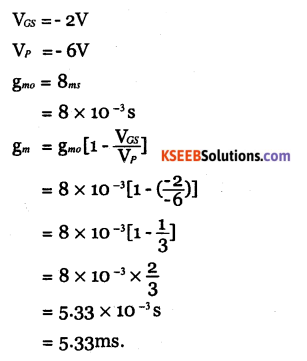
Question 5.
Find the value of gm, if VGS = -2V, Vp = – 6V, and gmo = 8 ms.
Answer: